EU Invests €15M to Help Companies Supercharge Their Products with Light (April 2025)
New investment from the European Commission is helping innovators exploit the unique properties
of light technologies to add smart features and improve the performance of their products through
a proven ‘one-stop-shop’ photonics innovation factory.
III-V Lab is honoured to be part of the new PhotonHub PHACTORY Consortium in delivering photonics-led
innovation support for the following industries: Defense & Space, Datacom-Telecom & Quantum telecommunications.
See the
press release
.
20 Years of Success: The Power of Collaboration and a Shared Vision in the Joint Lab of Thales, Nokia and CEA-Leti (Oct 2024)
Celebrating a Legacy of Collaboration, Excellence, and Recognition Across Multiple Fields, and a Role as a Key Contributor in the World
of Semiconductor Production
See the
press release and the
French press release.
Innovative semiconductor and packaging technologies up to 6G (June 2023)
Supported by 43 partners, the SHIFT project (Sustainable Technologies Enabling Future Telecom Applications) aims to make important
contributions to the "twin transition", through innovations in component and system technologies for advanced telecommunications.
See the
press release.
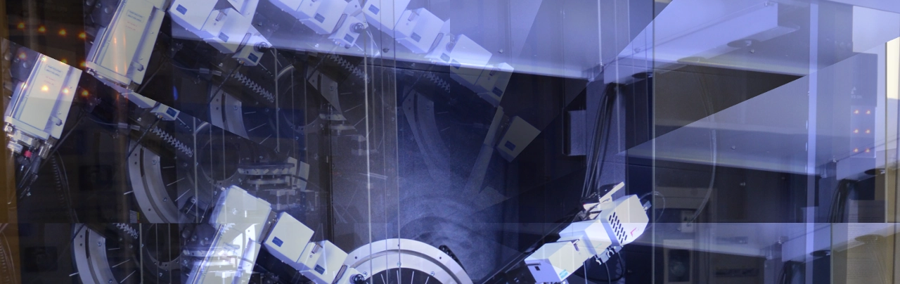
III-V Lab counts on RIBER’s equipments, with France Relance’s support, for the realization of photonic and nanoelectronic components of the future (February 2022)
III-V photonic and electronic component fabrication requires suitable, modular and scalable equipments. III-V materials, at the core of Telecom, Defence, Security and Spatial Systems,
are created atomic layer by atomic layer in epitaxy reactors.
By choosing the supplier Riber with France Relance’s support, III-V Lab is acquiring state-of-the-art epitaxy reactor for the realization of its advanced components.
See the
press release and the
French press release.
« European electro-optic and nonlinear PIC platform based on lithium niobate » (February 2022)
Launch of the ELENA project which will offer enhanced performance and new functionalities for these applications: telecoms, LIDAR, quantum technologies and microwave photonics.
This project has received funding from the European Union’s Horizon 2020 research and innovation program under grant agreement N° 101016138.
See the
French press release.
A leap in compactness and bandwidth, higher than 110 GHz, for a key telecommunications component opens the door to 6G at III-V Lab (November 2021)
The photodiode is a key component to increase the performance of telecommunications and in particular to cope with the continuous increase in traffic data.
Reaching a bandwidth greater than 110GHz, this ultra-compact, high-sensitivity photodiode provides a major breakthrough at III-V Lab
and Nokia Bell Labs, for 5G, and even makes it possible to reach the frequencies needed for 6G.
See the
press release and the
French press release.
PLAT4M Matures Three Silicon Photonic Platforms (July 2017)
Accelerates Commercialization of Technology by Linking the Silicon Photonic Ecosystem
III-V Lab has designed and co-fabricated a state-of-the-art integrated hybrid III-V/Si
transmitter using a wafer bonding technique, see the
press release.
The world's-first WVGA 10-µm pitch GaN microdisplays for augmented reality video (May 2017)
Presented at Display Week in Los Angeles, May 21-26
Leti will present that new technology at Display Week in an invited talk, “A Novel Process for Fabricating High-Resolution and Very Small Pixel-pitch GaN LED Microdisplays”.
The presentation at 5 p.m., May 23, will demonstrate the feasibility of LED arrays with pixel pitch as small as 3 µm, which is a world record.
These results, presented by Leti were obtained under III-V Lab collaborative workprogramme, see the
press release.
“Haute couture” photonics: (June 2016)
Almae technologies takes French excellence and innovation in nanoelectronics, led by III-V Lab, to an industrial scale
Almae technologies is commercializing an innovative photonic technology developed by teams from Nokia Bell Labs, Thales and the CEA at III-V Lab to address telecom and data storage center demands for high speed optical data transmission.
The startup has the industrial infrastructure to rapidly bring to market advanced components required to keep pace with the rapid growth in Internet data volumes.
See the press release and the French press release.
III-V Lab Partner in Silicon Photonics Supply-Chain Project (18 November 2015)
PLAT4M Project Focused on Speeding Industrialization of the Technology
III-V Lab have co-developed with Leti, integrated hybrid III-V lasers and electro-absorption modulators (EAM) on silicon using a wafer bonding technique,
confirming strong potentials for telecom applications.
See the
Press Release.
III-V Quantum dots & dashes on Silicon: a breakthrough towards efficient 16 x 25 Gb/s WDM photonic integrated circuits
Significant advances in silicon photonic integrated circuits (PICs) have been achieved in the European FP7 project SEQUOIA (energy efficient Silicon Emitter using heterogeneous integration of III-V QUantum dOt and quantum dash materIAls).
More information on the
press release.
Leti Demos New Process to Fabricate High-brightness Micro-LED Arrays for Next-gen Head-mounted and Head-up Displays (June 2015)
Gallium-nitride (GaN) and Indium Gallium-nitride (InGaN) Technology Targets Fast-growing Markets for Wearable Vision Systems
The high-density micro-LED array process was developed in collaboration with III-V Lab.
The high-brightness, enhanced-vision systems such as head-up and head-mounted
displays can improve safety and performance in fields such as aeronautics and
automotive, where the displays allow pilots and drivers to receive key navigation data
and information in their line of sight. For consumers, smart glasses or nomadic
projection devices with augmented reality provide directions, safety updates,
advertisements and other information across the viewing field. LED microdisplays are
ideally suited for such wearable systems because of their low footprint, low power
consumption, high-contrast ratio and ultra-high brightness.
More information on the
press release (and
french version).
mirSense signs infrared spectrometry agreement with Alcatel-Lucent, Thales and CEA-Leti (May 2015)
Alcatel-Lucent, Thales and CEA-Leti have signed a memorandum of understanding with mirSense, a start-up formed by Mathieu Carras and Mickael Brun, to market a disruptive technology developed by their joint research unit, III-V Lab.
mirSense will manufacture miniaturised tunable laser sources that are expected to revolutionise the infrared spectrometry market.
More information on the
press release.
Sofradir acquires infrared technologies from Safran and Thales (November 2012)
By acquiring the technologies of Safran, Thales and the GIE III-V Lab (Thales, Alcatel-Lucent, CEA), Sofradir consolidates French infrared (IR)
technologies under one roof, bolstering its capabilities in the imaging sector (
Press release).
Alcatel-Lucent Bell Labs, Thales and CEA-Leti join forces
to combine unique expertise in III-V semiconductors and silicon technologies (March 2011)
Enlarged partnership in III-V Lab will target applications in telecoms, industrial control, environmental testing, defence, security and space
Saclay, France, March 7, 2011 - Alcatel-Lucent Bell Labs, Thales and CEA-Leti today announced that CEA-Leti has joined the III-V Lab in a move to strengthen the industrial research capabilities of the R&D center, already Europe's most advanced in the field of III-V semiconductors. The new public-private partnership will combine III-V semiconductor and silicon technologies, opening up new research perspectives and dynamics. The enlarged III-V Lab will include more than 130 researchers, technicians, and doctoral candidates (
Press release and
French version)